Contact pad

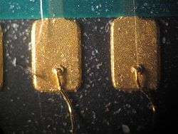
Gold wire ball-bonded to a gold contact pad
Contact pads are designated surface areas of a printed circuit board or die of an integrated circuit. Possibilities to contact to pads include soldering, wirebonding, flip chip mounting, or probe needles.
Further reading
- Jing Li, Evaluation and Improvement of the Robustness of a PCB Pad in a Lead-free Environment, ProQuest, 2007 ISBN 0-549-32110-1.
- Kraig Mitzner, Complete PCB Design Using OrCAD Capture and PCB Editor, Newnes, 2009 ISBN 0-08-094354-3.
- Deborah Lea, Fredirikus Jonck, Christopher Hunt, Solderability Measurements of PCB Pad Finishes and Geometries, National Physical Laboratory, 2001 OCLC 59500348.
This article is issued from Wikipedia - version of the 3/22/2016. The text is available under the Creative Commons Attribution/Share Alike but additional terms may apply for the media files.