Surface photovoltage
Surface photovoltage (SPV) measurements are a widely used method to determine the minority carrier diffusion length of semiconductors. Since the transport of minority carriers determines the behavior of the p-n junctions that are ubiquitous in semiconductor devices, surface photovoltage data can be very helpful in understanding their performance. As a contactless method, SPV is a popular technique for characterizing poorly understood compound semiconductors where the fabrication of ohmic contacts or special device structures may be difficult.
Theory

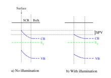
As the name suggests, SPV measurements involve monitoring the potential of a semiconductor surface while generating electron-hole pairs with a light source. The surfaces of semiconductors are often depletion regions (or space charge regions) where a built-in electric field due to defects has swept out mobile charge carriers. A reduced carrier density means that the electronic energy band of the majority carriers is bent away from the Fermi level. This band-bending gives rise to a surface potential. When a light source creates electron-hole pairs deep within the semiconductor, they must diffuse through the bulk before reaching the surface depletion region. The photogenerated minority carriers have a shorter diffusion length than the much more numerous majority carriers, with which they can radiatively recombine. The change in surface potential upon illumination is therefore a measure of the ability of minority carriers to reach the surface, namely the minority carrier diffusion length. As always in diffusive processes, the diffusion length is approximately related to the lifetime by the expression , where is the diffusion coefficient. The diffusion length is independent of any built-in fields in contrast to the drift behavior of the carriers.
Note that the photogenerated majority carriers will also diffuse towards the surface but their number as a fraction of the thermally generated majority carrier density in a moderately doped semiconductor will be too small to create a measurable photovoltage. Both carrier types will also diffuse towards the rear contact where their collection can confuse interpretation of the data when the diffusion lengths are larger than the film thickness. In a real semiconductor, the measured diffusion length includes the effect of surface recombination, which is best understood through its effect on carrier lifetime:
where is the effective carrier lifetime, is the bulk carrier lifetime, is the surface recombination velocity and is the film or wafer thickness. Even for well characterized materials, uncertainty about the value of the surface recombination velocity reduces the accuracy with which the diffusion length can be determined for thinner films.
Experimental methods

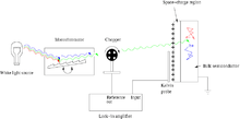
Surface photovoltage measurements are performed by placing a wafer or sheet film of a semiconducting material on a ground electrode and positioning a kelvin probe a small distance above the sample. The surface is illuminated with light whose wavelength is scanned using a monochromator so as to vary the absorption depth of the photons. The deeper in the semiconductor that carrier generation occurs, the fewer the number of minority carriers that will reach the surface and the smaller the photovoltage. On a semiconductor whose spectral absorption coefficient is known, the minority carrier diffusion length can in principle be extracted from a measurement of photovoltage versus wavelength. The optical properties of a novel semiconductor may not be well known or may not be homogeneous across the sample. The temperature of the semiconductor must be carefully controlled during an SPV measurement test thermal drift complicate the comparison of different samples. Typically SPV measurements are done in an AC-coupled fashion using a chopped light source rather than a vibrating Kelvin probe.
Significance
The minority carrier diffusion length is critical in determining the performance of devices such as photoconducting detectors and bipolar transistors. In both cases the ratio of the diffusion length to the device dimensions determines the gain. In photovoltaic devices, photodiodes and field-effect transistors, the drift behavior due to built-in fields is more important under typical conditions than the diffusive behavior. Even so the SPV is a convenient method of measuring the density of impurity-derived recombination centers that limit device performance. SPV is performed both as an automated and routine test of material quality in a production environment and as an experimental tool to probe the behavior of less well studied semiconducting materials. Time-resolved photoluminescence is an alternate contactless method of determining minority carrier transport properties.
See also
References
- Schroder, Dieter K. (2006). Semiconductor Material and Device Characterization. Wiley-IEEE Press. ISBN 0-471-73906-5.
- Schroder, Dieter K. (2001). "Surface voltage and surface photovoltage: history, theory and applications". Meas. Sci. Techn. 12 (3): R16. Bibcode:2001MeScT..12R..16S. doi:10.1088/0957-0233/12/3/202.
- Kronik, L.; Shapira, Y. (1999). "Surface photovoltage phenomena: theory, experiment, and applications" (PDF). Surface Science Reports. 37: 1–206. Bibcode:1999SurSR..37....1K. doi:10.1016/S0167-5729(99)00002-3. Archived from the original (PDF) on 2005-03-12. Retrieved 2008-07-03.
External links
- Semilab vendor of commercial SPV and Minority Carrier Lifetime measurement systems
- KP Technology vendors of and consultants about Kelvin probes
- ASTM standard F391-96 "Standard Test Methods for Minority Carrier Diffusion Length in Extrinsic Semiconductors by Measurement of Steady-State Surface Photovoltage"