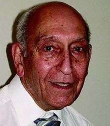
Sorab K. Ghandhi
| Sorab K Ghandhi | |
|---|---|
 | |
| Born |
January 1, 1928 Allahabad, India |
| Residence | Escondido, CA |
| Nationality | United States of America |
| Alma mater | University of Illinois |
| Occupation | Professor Emeritus at Rensselaer Polytechnic Institute |
| Spouse(s) | Cecilia M. Ghandhi |
| Children | Khushro, Rustom, Behram |
Sorab (Soli) K. Ghandhi (born 1928) is a professor Emeritus at Rensselaer Polytechnic Institute (RPI) known for his pioneering work in electrical engineering and microelectronics education, and in the research and development of Organometallic Vapor Phase Epitaxy (OMVPE) for compound semiconductors. He was the recipient of the IEEE Education Award "For pioneering contributions to semiconductor and microelectronics education" in 2010.
Education
Ghandhi was schooled at St. Joseph's College, Nainital, India, received his B.Sc. in electrical and mechanical engineering from Benares Hindu University in 1947, and his MS and Ph.D. in electronics from the University of Illinois in 1948 and 1951 respectively. He is a Zoroastrian by birth, and has three sons, Khushro, Rustom and Behram.
Career
While a member of the Advanced Circuits Group, General Electric Company, from 1951–1960, he co-authored the first books in the world on transistor circuits[1] and transistor circuit engineering[2] He was a manager of the Components Group at the Philco Corporation from 1960-1963. During this time, as Chairman of the IRE Standards on Graphical symbols,Task Group 28.4.8, he was instrumental in obtaining international adoption of the US-derived graphical symbol for Transistors and other Semiconductor devices.[3] He joined Rensselaer Polytechnic Institute (RPI) in 1963 as a Professor of Electrophysics, and was Chairman from 1967-1974. He retired from RPI in 1992.
At RPI, he introduced microelectronics into the graduate studies curriculum and wrote a book on this subject.[4] This was the first book in the world to elucidate the necessary background required for an engineer to participate in the semiconductor industry. In addition to basic semiconductor physics, it covered topics such as Crystal Growth, Phase Diagrams, Diffusion, Oxidation, Epitaxy, Etching and Photolithography, which were not typical of the background of electrical engineers. Subsequently, this was followed by a book on semiconductor power devices,[5] in which he presented a comprehensive theory for second breakdown. Following the work of Manasevit in 1968,[6] he started the first university program on the OMVPE of compound semiconductors in 1970, and conducted research with his students in this area until retirement. This technology has become increasingly popular, and is now used in most modern optical devices such as lasers and light emitting diodes, transmitters and receivers for fiber optic communications and improved thermoelectric structures.
His research in OMVPE included the growth and characterization of GaAs,[7] InAs, GaInAs, InP, CdTe, HgCdTe and ZnSe materials and devices, which resulted in over 180 papers. Many of these were "firsts" in the field: the growth of GaInAs over the full range of compositions,[8] the use of homostructures for evaluating recombination in surface-free GaAs,[9] the use of halogen etching in GaAs,[10] the OMVPE growth of large area films of HgCdTe with highly uniform composition[11] and the p-type doping of this HgCdTe.[12]
Concurrent with his research activities, he also wrote two books on VLSI fabrication principles which included a comprehensive, unified treatment of Silicon and GaAs materials technology.[13] and a [14] These covered, for the first time, topics relevant to Compound Semiconductors, which are increasingly playing an important role in advanced semiconductor electro-optical and communication devices and systems.
Membership
- Member, Administrative Committee, IEE Transactions on Circuit Theory (1963-1966)
- Guest Editor, Special Issue of the IEEE on Materials and Processes in Microelectronics (1966–1967)
- Associate Editor, Solid-State Electronics (1974–1988)
- Secretary, International Solid State Circuits Conference (1959)
- Program Chairman, International Solid State Circuits Conference (1960)
- Co-Chairman, Workshop on HgCdTe and other Low Gap Materials (1992)
- Member, Editorial Board, IEEE Press (1983-1987).
Awards
- Scholar, J.N. Tata Foundation (1947-1951)
- Fellow, IEEE (1965)[15]
- Rensselaer Distinguished Teaching Award (1975)
- Rensselaer Distinguished Professor Award (1987)
- Education Award, Electron Device Society, IEEE (2010)[16]
References
- ↑ Principles of Transistor Circuits, (Ed.R.F. Shea). John Wiley and Sons. 1953. pp. 535.
- ↑ Transistor Circuit Engineering, (Ed.R.F. Shea). John Wiley and Sons. 1957. pp. 468
- ↑ http://www.ieeeghn.org/wiki/index.php/First-Hand:Saving_the_Transistor_Symbol
- ↑ Theory and Practice of Microelectronics, John Wiley and Sons. 1968. pp.487.
- ↑ Semiconductor Power Devices, John Wiley and Sons. 1977.pp.329.
- ↑ H.M. Manasevit and W.J. Simpson, "The use of Metal-Organics in the Preparation of Semiconductor Materials: I. Epitaxial Gallium-V Compounds", J. Electrochem. Soc. 116, 1725. (1969).
- ↑ D.H. Reep and S.K. Ghandhi, "Deposition of GaAs Epitaxial Layers by Organometallic CVD. J. Electrochem. Soc. 130, 675 (1983).
- ↑ . B. Jayant Baliga and Sorab K. Ghandhi, "Growth and Properties of heteroepitaxial GaInAs Alloys on GaAs Substrates using Trimethylgallium, Triethylindium, and Arsine", J. Electrochem. Soc. 122, 1725 (1975).
- ↑ L.M. Smith, D.J. Wolford, R. Venkatasubramanian and S.K. Ghandhi, "Radiative Recombination in Surface-Free n+n-n+ Homostructures", Appl. Phys. Lett. 57 1572 (1990)
- ↑ R. Bhat and S.K. Ghandhi, "The Effect of Chloride Etching on GaAs Epitaxy using TMG and Arsine", J. Electrochem Soc. 125, 771, (1978).
- ↑ Sorab K. Ghandhi, Ishwara B. Bhat and Hamid Fardi, "Organometallic Epitaxy of HgCdTe on CdTeSe substrates with high compositional uniformity", Appl. Phys. Lett. 52 (5), 392 (1988).
- ↑ S.K. Ghandhi, N.R. Taskar, K.K. Parat, D. Terry and I.B. Bhat, "Extrinsic p-type doping of HgCdTe grown by Organometallic Epitaxy", Appl. Phys. Lett. 53 (17), 392 (1988).
- ↑ VLSI Fabrication Principles: Silicon and Gallium Arsenide, John Wiley and Sons. 1983. pp. 665.
- ↑ Completely Revised Edition, VLSI Fabrication Principles: Silicon and Gallium Arsenide, John Wiley and Sons. 1994. pp.834.
- ↑ http://www.ieee.org/membership_services/membership/fellows/chronology/fellows_1965.html
- ↑ "IEEE Education Awards". Retrieved 1 April 2012.
